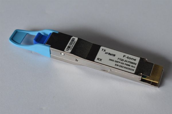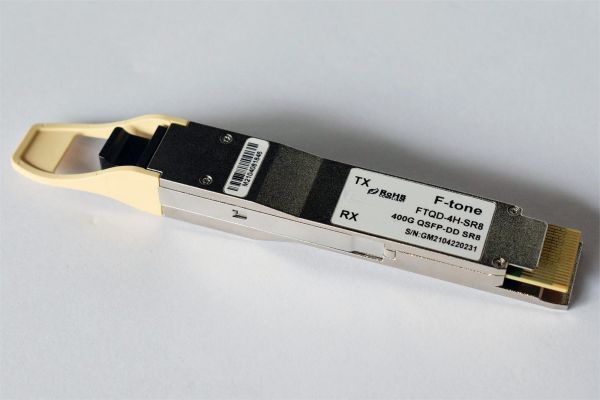
Description
The 400G QSFP-DD ZR Transceiver is a high performance, cost effective module for optical data communication applications from 100G to 400G. The 400G QSFP-DD ZR+ is designed to 100G/200G long haul and 300G/400G Metro IP over DWDM applications without inline chromatic dispersion compensation.
The 400G QSFP-DD ZR+ is a C-Band optical frequency tunable coherent optical module, combines 7nm coherent DSP ASIC functionality with best in class ultra-narrow line-width tunable lasers, high speed modulators and high responsively coherent receivers to deliver high performance at 100G DP-QPSK / 200G DP-QPSK / 300G DP-8QAM / 400G DP-16QAM modulation format. With one VOA inside the TX optical path the out output optical power has 4dB attenuation window.
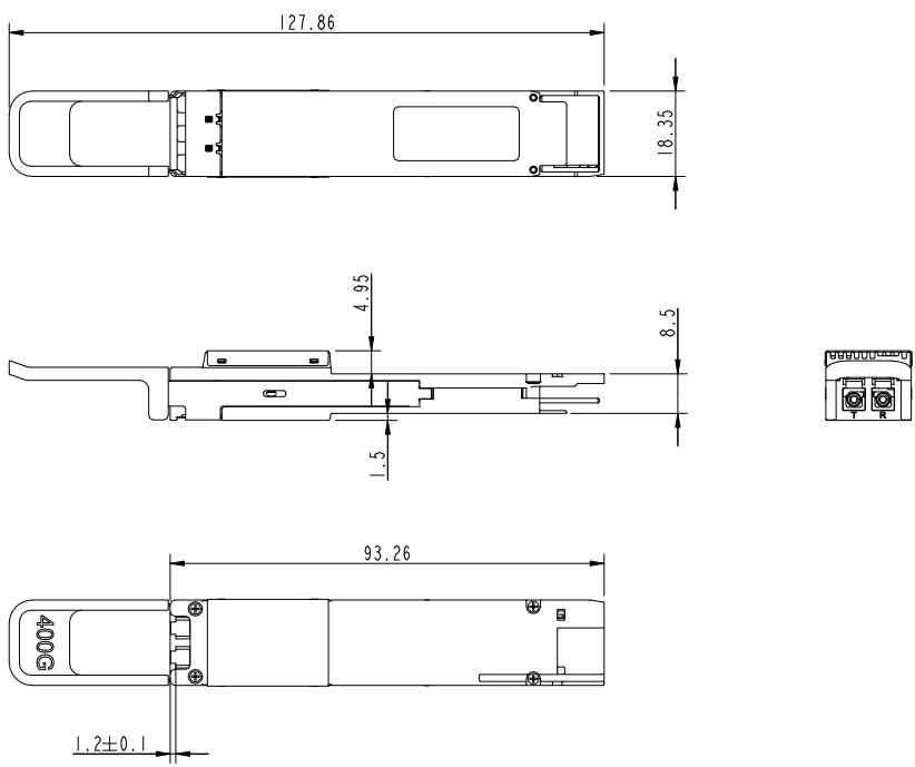
The 400G QSFP-DD ZR+ coherent transceiver Compliant with the OIF QSFP-DD MSA. Digital diagnostics functions are available via an I2C interface as specified by the QSFP-DD MSA. Mechanical dimensions, connectors and footprint conform to QSFP-DD MSA. The module is 18.35mm x93.26mmx8.50mmin size and hot pluggable by 76 PIN PAD and host connector.
Features
● Compliant with QSFP-DD MSA, Type 2B package
● Compliant with Open ZR+ MSA and OIF 400ZR MSA, support OFEC and CFEC FEC
● Line rate 100G/200G/300G/400G
● Client rate 1/2/3/4x100GbE or 1x400GbE
● C-band tunable, supports 100/75/50GHz grid spacing, support 0.1GHz fine turning
● TX VOA inside, with 4dB attenuation window
● Support ingress LF hold-off time configure
● Support hitless firmware upgrade
● Compact size (18.35 mm x 93.26 mm x 8.50 mm)
● Duplex LC connector
● Operating case temperature: 0℃ to 75°C
● Single 3.3 V power supply
● Typical power consumption 21W (400GbE),maximum power consumption 22.5W(400GbE)
● RoHS 2 compliant
Applications
● Edge DCI with extended Reach or with OLP protection
● IP Over Metro or Long Haul DWDM
Compliance
● Open ZR+ MSA 2.0 and OIF-400ZR-02.0
● OIF-CMIS-05.2
● IA OIF-C-CMIS-01.2
● QSFP-DD-Hardware-Rev6.3
● IEEE Std 802.3-2018
Absolute Maximum Ratings
Table1-Absolute Maximum Ratings
| Parameter | Symbol | Min. | Typ. | Max. | Unit | Note |
| Storage temperature | Ts | -40 | 85 | ℃ | ||
| Power supply | Vcc | -0.3 | 3.3 | 3.6 | V | not damaged |
| Relative humidity | RH | 5 | 85 | % | Non-condensing | |
| Receiver damage threshold | PRdmg | 10 | dBm | Total optical power | ||
| ESD Sensitivity | 1000 | V |
Recommended Operating Conditions
Table2-Recommended Operating Conditions
| Parameter | Symbol | Min. | Typ. | Max. | Unit | Note | |
| Operating Case Temperature | TC | 0 | 75 | ℃ | |||
| Power supply voltage | VCC | 3.135 | 3.3 | 3.465 | V | ||
| ICC | 7.2 | A | Note1 | ||||
| Maximum sustained peak Current(<500ms) | 7.4 | A | |||||
| Maximum Instantaneous peak current(<50us) | 9 | A | |||||
| Electro-Static discharge | ESD | 1000 | V | ||||
| Power Consumption(400ZR+) | PD | 21 | 22.5 | W | Note1 | ||
| Relative humidity | RH | 15 | 85 | % | |||
| Client Mode | 400G (400ZR) | 1 x 400GAUI-8 | |||||
| 4 x 100GAUI-2 | |||||||
| 400G (400ZR+) | 1 x 400GAUI-8 | ||||||
| 4 x 100GAUI-2 | |||||||
| 300G (300ZR+) | 3 x 100GAUI-2 | ||||||
| 200G (200ZR+) | 2 x 100GAUI-2 | ||||||
| 2 x CAUI-4 | Note2 | ||||||
| 100G (100ZR+) | 1 x 100GAUI-2 | ||||||
| 1 x CAUI-4 | Note2 | ||||||
| Transmissi onDistance | 400G (OIF 400ZR app code 0x01) | 120 | Km | ||||
| 400G (OIF 400ZR app code 0x02) | 30~40 | ||||||
| 400G (400ZR+) | 450 | ||||||
| 300G (300ZR+) | 600 | ||||||
| 200G (200ZR+) | 1000 | ||||||
| 100G (100ZR+) | 2000 | ||||||
| Power Supply Noise | Vrip | 1% | DC-1MHz | ||||
| 2% | 1-10MHz | ||||||
Notes
[1] In 400GbE mode, the typical power consumption is 21W and the maximum power consumption is 22.5W .When switching to 4×100GbE mode , the typical power consumption will be 22W and the maximum power consumption will be 23W, the current will also change accordingly.
[2] Not tested in standard PN. Will be supported upon customer request.
Optical ,Electrical Characteristic
Tested under recommended operating conditions, unless otherwise noted Table3-Transmitter Operating Characteristic-Optical ,Electrical
| Parameters | Unit | Min. | Type | Max. | Note | |
| Modulation format | 400G | ZR400-CFEC-16QAM | CFEC FEC, NCG 10.8dB | |||
| ZR400-OFEC-16QAM | OFEC FEC, NCG 11.6dB | |||||
| 300G | ZR300-OFEC-8QAM | |||||
| 200G | ZR200-OFEC-QPSK | |||||
| 100G | ZR100-OFEC-QPSK | |||||
| Baud Rate | 400G | GBd | 59.843750000±20ppm | 400ZR,SFF-8024 Media ID 3Eh/3Fh | ||
| 60.138546798±20ppm | 400ZR+,SFF-8024 Media ID 46h | |||||
| 300G | 60.138546798±20ppm | 300ZR+,SFF-8024 Media ID 47h | ||||
| 200G | 60.138546798±20ppm | 200ZR+,SFF-8024 Media ID 48h | ||||
| 100G | 30.069273399±20ppm | 100ZR+, SFF-8024 Media ID 49h | ||||
| Transmitter frequency range | THz | 191.3 | 196.1 | For OIF 400ZR app code 0x02 the frequency is fixed at 193.7THz and not configurable. | ||
| Flexible DWDM Grid | GHz | 3.125 | ||||
| Frequency Fine Tuning range | GHz | -5 | 5 | bright tuning | ||
| Frequency Fine Tuning step | GHz | 0.1 | ||||
| Laser frequency accuracy | GHz | -1.8 | 1.8 | |||
| TX spectral Upper Mask | (GHz,dB) | (30.0,0.0)(37.0,-10.0)(39.2,-15.0)(40.4,-20.0) | Refer to OIF-400ZR-02.0 13.3.201a Refer to openzrplus_2p0 11.4.10 | |||
| TX spectral Lower Mask | (GHz,dB) | (30.0,-9.0)(31.3,-20.0)(31.3,-3 | Refer to OIF-400ZR-02.0 13.3.201b Refer to openzrplus_2p0 11.4.10 | |||
| 5.0) | ||||||
| Transmitter laser disable time | ms | 100 | ||||
| Transmitter wavelength switching time | s | 60 | ||||
| Transmitter laser enable time | s | 10 | ||||
| Tx output power | 400G | dBm | -10 | -6 | At Programmed Output Power Max,Transmit output power overwavelength, temperature, and aging. | |
| 300G | dBm | -10 | -6 | |||
| 200G | dBm | -9 | -5 | |||
| 100G | dBm | -8 | -4 | |||
| Transmit Output Power at 400G ZR Gray | dBm | -9 | -6 | For OIF 400ZR app code 0x02 | ||
| Transmit Output Power Adjustable Range | 400G 300G | dBm | -13 | -9 | The absolute accuracy is ±1dBFor OIF 400ZR app code 0x02 the output power is not configurable. | |
| Transmit Output Power Adjust step | dB | 0.1 | ||||
| Optical power setting accuracy | dB | -1 | 1 | Diff between setting and reporting | ||
| Output power monitor accuracy | dB | -1 | 1 | |||
| Power stability | dB | -0.5 | 0.5 | At fixed wavelength, room temp | ||
| -1 | 1 | At fixed wavelength | ||||
| Total output power with Tx disabled | dBm | -20 | ||||
| Total output power during wavelength switching | dBm | -20 | ||||
| Transmitter reflectance | dB | -20 | Looking into the Tx | |||
| Inband (IB) OSNR | dB | 40 | ||||
| Out-of-band (OOB) OSNR | dB | 35 | ||||
| Lorentzian linewidth | kHz | 300 | Tx and LO | |||
| Relative intensity noise | dB/Hz | -140 | ||||
| Mean I-Q amplitude imbalance | dB | 1 | ||||
| Transmitter polarization dependent power | dB | 1.5 | ||||
| DC I-Q offset (mean perpolarization) | dB | -26 | ||||
| I-Q instantaneous offset | dB | -20 | ||||
Table4- Receiver Operating Characteristic-Optical
| Parameters | Unit | Min. | Type | Max. | Note | |||
| Modulation format | 400G | ZR400-CFEC-16QAM | CFEC FEC,Net Coding Gain(NCG) 10.8dB,Theoretical Max Pre-FEC BER 1.25E-2 | |||||
| ZR400-OFEC-16QAM | OFEC FEC,Net CodingGain(NCG) 11.6dB ,Theoretical | |||||||
| 300G | ZR300-OFEC-8QAM | |||||||
| 200G | ZR200-OFEC-QPSK | Max Pre-FEC BER 2.0E-2 | ||||||
| 100G | ZR100-OFEC-QPSK | |||||||
| Baud Rate | 400G | GBd | 59.843750000±20ppm | 400ZR,SFF-8024 Media ID 3Eh/3Fh | ||||
| 60.138546798±20ppm | 400ZR+,SFF-8024 Media ID 46h | |||||||
| 300G | 60.138546798±20ppm | 300ZR+,SFF-8024 Media ID 47h | ||||||
| 200G | 60.138546798±20ppm | 200ZR+,SFF-8024 Media ID 48h | ||||||
| 100G | 30.069273399±20ppm | 100ZR+,SFF-8024 Media ID 49h | ||||||
| Frequency offset between received carrier and LO | GHz | -3.6 | +3.6 | |||||
| Input power range | 400G | dBm | -12 | 0 | Signal power,OSNR>26dB,400ZR | |||
| -12 | 0 | Signal power,OSNR>24dB, 400ZR+ | ||||||
| 300G | -15 | 0 | Signal power,OSNR>21dB, 300ZR+ | |||||
| 200G | -18 | 0 | Signal power, OSNR>16dB, 200ZR+ | |||||
| 100G | -18 | 0 | Signal power, OSNR>12.5dB,100ZR+ | |||||
| OSNR Tolerance | 400G | dB/0.1n m | 26 | 400ZR | Measured back-to-back with short optical channel | |||
| 24 | 400ZR+ | |||||||
| 300G | 21 | 300ZR+ | ||||||
| 200G | 16 | 200ZR+ | ||||||
| 100G | 12.5 | 100ZR+ | ||||||
| RX sensitivity | 400G | dBm | -20 | 400ZR | Inband (IB) OSNR ≥ 34dB, OIF 400ZR app code 0x02 | |||
| -22 | 400ZR+ | Point to point | ||||||
| non-damaging input power | dBm | 10 | Total power | |||||
| Optical input power monitor accuracy | dB | -2 | 2 | Total power | ||||
| MAX Pre-FEC BER | 0.017 | 0.020 | ||||||
| Chromatic dispersion tolerance | 400G | ps/nm | 2,400 | 400ZR | Tolerance to CD with ≤ 0.5 dB penalty to OSNR sensitivity when change in SOP is ≤ 1rad/ms | |||
| 20,000 | 400ZR+ | |||||||
| 300G | 40,000 | 300ZR+ | ||||||
| 200G | 50,000 | 200ZR+ | ||||||
| 100G | 100,000 | 100ZR+ | ||||||
| CD monitor accuracy | ps/nm | -200 | +200 | |||||
| DGD tolerance | 400G | ps | 33 | 400ZR | OSNR penalty<0.5dB | |||
| 66 | 400ZR+ | |||||||
| 300G | 83 | 300ZR+ | ||||||
| 200G | 83 | 200ZR+ | ||||||
| 100G | 100 | 100ZR+ | ||||||
| DGD monitor accuracy | ps | -15 | 15 | 0~40ps for 400ZR 0~100ps for 400/300/200/100ZR+ | ||||
| Peak PDL tolerance | dB | 3.0 | Tolerance to peak PDL with ≤1.3dB additional OSNR penalty when change in SOP is ≤1 rad/ms | |||||
| 3.5 | Tolerance to peak PDL with ≤1.8dB additional OSNR penalty when change in SOP is ≤1 rad/ms | |||||||
| Tolerance to change in SOP | krad/s | 50 | With ≤0.5dB additional OSNR penalty over all PMD and PDL values | |||||
| Optical return loss | dB | 20 | Optical reflectance at Rx connector input. | |||||
| Optical Rx_LOS Assert Threshold | 400G | dBm | -28 | -26 | -24 | OIF 400ZR app code 0x01 ,0x02, 0x03, | ||
| 400G | -30 | -28 | -26 | 400ZR+ | ||||
| 300G | -32 | -30 | -28 | |||||
| 200G | -32 | -30 | -28 | |||||
| 100G | -32 | -30 | -28 | |||||
| Optical Rx_LOS Hysteresis | dB | 1 | 1.5 | 2.5 | ||||
| Optical input power transient tolerance | dB | -2 | 2 | Tolerance to change in input power with<0.5dB penalty to OSNR tolerance.The 20% to 80% rise/fall times for the input power change shall be no faster than 50 µs. | ||||
| Service recovery time | ms | 40 | ||||||
The transmitter and receiver comply with the 400GAUI-8 C2M and CEI-56G-VSR-PAM4 electrical specification, electrical interface definitions refer to IEEE Std 802.3-2018 Annex 120E. The data lines are AC-coupled and terminated in the module per the following figure from the QSFP-DD MSA.
Table5-Operating Characteristic-Electrical highspeed
| Parameter | Symbol | Min | Max | Unit | note |
| 400GAUI-8 C2M and 100GAUI-2 C2M Electrical Characteristics | |||||
| Transmitter(module output) | |||||
| Signaling Rate, each lane | 26.5625 ± 100 ppm | GBd | PAM-4 | ||
| AC common-mode output voltage (RMS) | RMS | 17.5 | mV | ||
| Differential Voltage pk-pk | Vin, pp | 750 | 900 | mV | |
| Near-end ESMW (Eye symmetry mask width) | 0.265 | UI | |||
| Near-end Eye height, differential | 70 | mV | |||
| Far-end ESMW | 0.2 | UI | |||
| Far-end Eye height,differential | 30 | mV | |||
| Far-end pre-cursor ISI ratio | -4.5 | 2.5 | % | ||
| Differential output return loss | Equation (83E-2) | IEEE Std 802.3-2018 Annex 120E | |||
| Common to differential mode conversion return loss | Equation (83E-3) | IEEE Std 802.3-2018 Annex 120E | |||
| Differential termination mismatch | – | 10 | % | At 1 MHz | |
| Transition time(20% to 80%) | Trise/Tfall | 9.5 | Ps | 20% to 80% | |
| DC common mode voltage | Vcm | -350 | 2850 | mV | |
| Receiver (module input) | |||||
| Signaling rate per lane | 26.5625 ± 100 ppm | GBd | PAM-4 | ||
| Differential pk-pk input voltage tolerance | Vout, pp | 900 | mV | ||
| Differential input return loss (min) | Equation (83E–5) | IEEE Std 802.3-2018 Annex 120E | |||
| Differential to common-mode input return loss (min) | Equation (83E–6) | IEEE Std 802.3-2018 Annex 120E | |||
| Differential termination mismatch | 10 | % | |||
| Module stressed input test | See 120E.3.4.1 | IEEE Std 802.3-2018 Annex 120E | |||
| Single-ended voltage tolerance range (min) | -0.4 | 3.3 | V | ||
| DC common mode voltage(min) | -350 | 2850 | mV | ||
| CAUI-4 C2M Electrical Characteristics | |||||
| Transmitter(module output) | |||||
| Signaling Rate, each lane | 25.78125 ± 100 ppm | GBd | NRZ | ||
| AC common-mode output voltage (RMS) | RMS | 17.5 | mV | ||
| Differential Voltage pk-pk | Vin, pp | 750 | 900 | mV | |
| Eye width | UI | 0.57 | |||
| Eye height, differentia | mV | 228 | |||
| Vertical eye closure | dB | 5.5 | |||
| Differential output return loss | Equation (83E-2) | IEEE Std 802.3-2018 Annex 83E | |||
| Common to differential mode conversion return loss | Equation (83E-3) | IEEE Std 802.3-2018 Annex 83E | |||
| Differential termination mismatch | – | 10 | % | At 1 MHz | |
| Transition time(20% to 80%) | Trise/Tfall | 12 | Ps | 20% to 80% | |
| DC common mode voltage | Vcm | -350 | 2850 | mV | |
| Receiver (module input) | |||||
| Signaling rate per lane | 25.78125 ± 100 ppm | GBd | NRZ | ||
| Differential pk-pk input voltage tolerance | Vout, pp | 900 | mV | ||
| Differential input return loss (min) | Equation (83E–5) | IEEE Std 802.3-2018 Annex 83E | |||
| Differential to common-mode input return loss (min) | Equation (83E–6) | IEEE Std 802.3-2018 Annex 83E | |||
| Differential termination mismatch | 10 | % | IEEE Std 802.3-2018 Annex 83E | ||
| Module stressed input test | See 83E.3.4.1 | ||||
| Single-ended voltage tolerance range (min) | -0.4 | 3.3 | V | ||
| DC common mode voltage(min) | -350 | 2850 | mV | ||
Table6-Operating Characteristic-Electrical Lowspeed
| Parameters | Symbol | Unit | Min. | Max. | Note |
| SCL and SDA | VOL | 0 | 0.4 | V | IOL(max)=3mA for fast mode, 20ma for Fast-mode plus |
| VOH | Vcc-0.5 | Vcc+0.3 | V | ||
| SCL and SDA | VIL | -0.3 | Vcc*0.3 | V | |
| VIH | VCC*0.7 | Vcc+0.5 | V | ||
| Capacitance for SCL and SDA I/O signal | Ci | 14 | pF | ||
| Total bus capacitivel oad for SCL and SDA | Cb | 100 | pF | For 400kHz clock rate, use 3.0 k Ohms pull up resistor max. For 1000kHz clock rate, refer to Figure 45 (QSFP-DD-Hardware-rev5p0) | |
| 200 | pF | For 400kHz clock rate, use 1.6 k Ohms pull up resistor max. For 1000kHz clock rate, refer to Figure 45 (QSFP-DD-Hardware-rev5p0) | |||
| InitMode, ResetL and ModSelLIntL | VIL | -0.3 | 0.8 | V | |
| VIH | 2 | VCC+0.3 | V | ||
| |Iin| | 360 | uA | 0V<Vin<Vcc | ||
| VOL | 0 | 0.4 | V | IOL=2.0mA | |
| VOH | VCC-0.5 | VCC+0.3 | V | 10k ohms pull up to Host Vcc | |
| ModPrsL | VOL | 0 | 0.4 | V | IOL=2.0mA |
| VOH | ModPrsL can be implemented as a short-circuit to GND on the module |
Dimensions
Ordering Information
| Part No. | Specification | Application | ||||||
| Pack | Rate | Tx/RX | Pout | Top | Reach | Others | ||
| FTQD-4H-ZR | QSFP-DD | 400G1 | ICTR | -10~-6dBm | 0~75℃ | 450km1 | DDM/ RoHS | 400G ZR+ |
北亿纤通 | F-tone Networks
企业邮箱: sales@f-tone.com
企业手机:19081343401
企业电话:028-85255257
企业传真:028-85977702
注:本产品有全国产化型号可选
本产品为QSFP-DD光模块,仅展示部分参数,如有需要,请联系我们。
Important Notice
Performance figures, data and any illustrative material provided in this data sheet are typical and must be specifically confirmed in writing by F-tone Networks before they become applicable to any particular order or contract. In accordance with the F-tone Networks policy of continuous improvement specifications may change without notice.
The publication of information in this data sheet does not imply freedom from patent or other protective rights of F-tone Networks or others. Further details are available from any F-tone Networks sales representative.
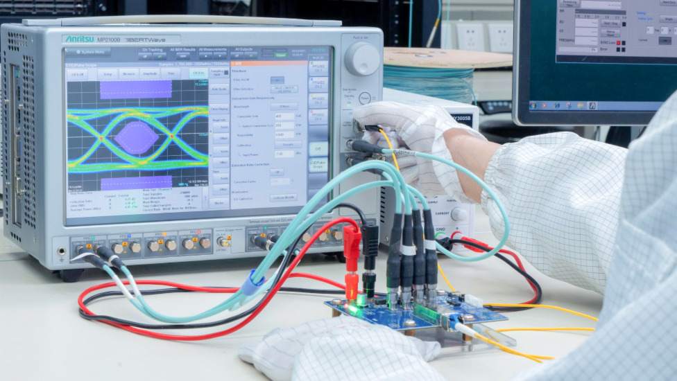
光学性能测试
测试光纤收发模块的眼图情况、接收灵敏度、消光比、波长、发光、光接收、电流和电压,以确保信号质量、传输的稳定性和可靠性。
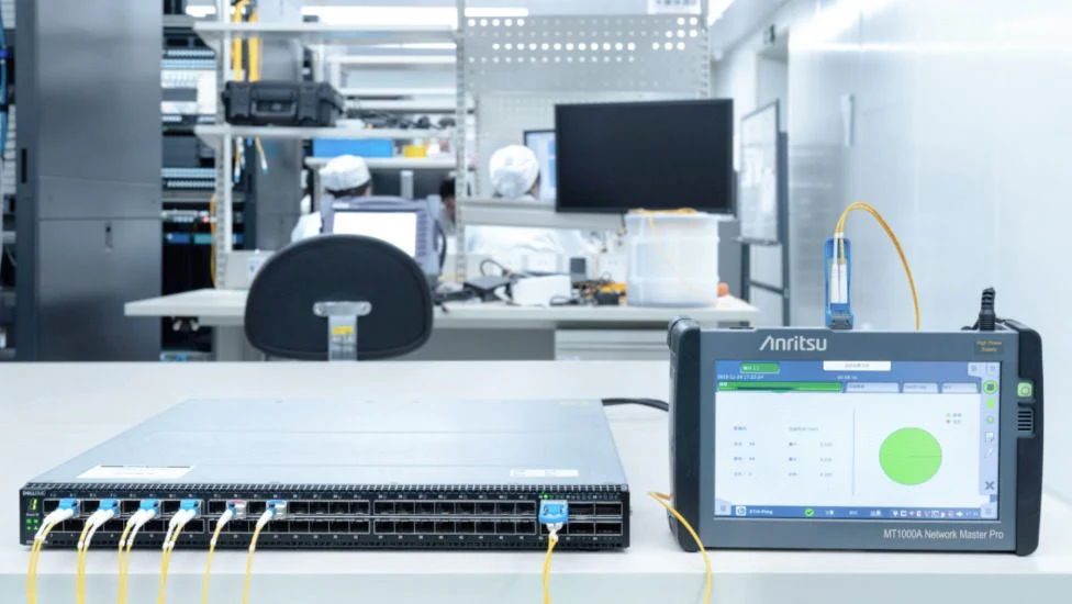
Traffic Testing
测试误码率和丢包率,使其符合相应标准,确保收发器的性能。
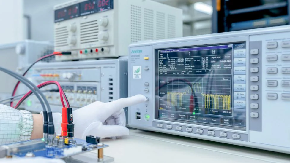
光学性能测试
测试光纤收发模块的眼图情况、接收灵敏度、消光比、波长、发光、光接收、电流和电压,以确保信号质量、传输的稳定性和可靠性。
端面测试
检查光纤收发模块的端面并保持清洁,以实现更稳定的数据传输、更好的性能和耐用性。

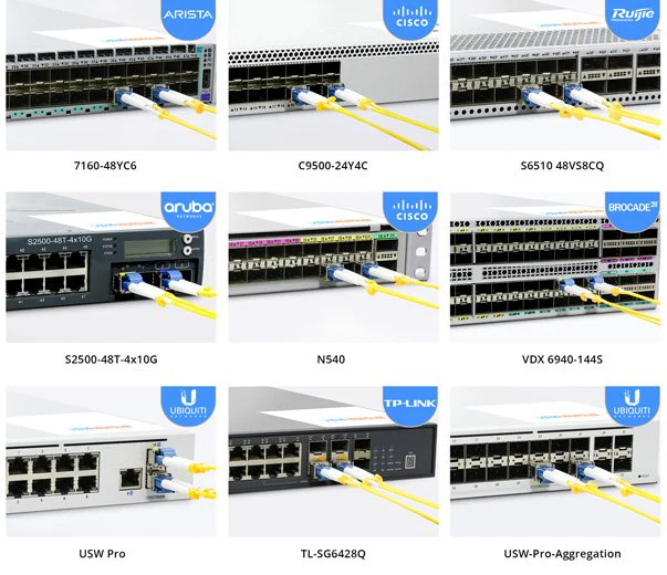
兼容品牌:
华为 | 华三 | 中兴 | 锐捷 | Cisco | Juniper | Arista | Brocade |HPE ProCurve | HPE Aruba | HPE BladeSystem | HPE H3C | H3C | Dell | Extreme | HW | Generic | F-tone | Intel | Netgear | IBM | NVIDIA/Mellanox (Ethernet) | Ciena | Fortinet | Avago | Avaya | Alcatel-Lucent | D-Link | F5 | Ubiquiti | Mikrotik |Broadcom…..