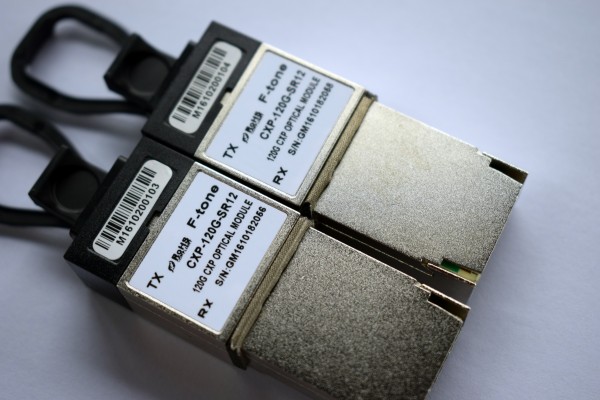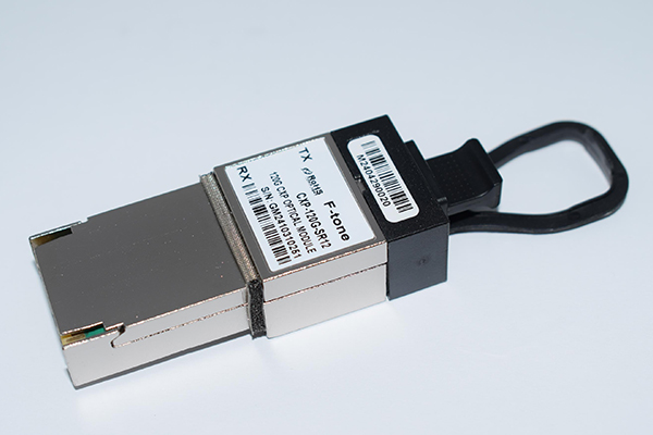
Description
F-tone Networks’s FTXP-H2-SR10xx CXP transceiver modules is a high performance, low power consumption, long reach interconnect solution supporting 100G Ethernet, Infiniband QDR,DDR,SDR,1G/2G/4G/8G/10G fiber channel and PCIe. It is compliant with the 120Gbits Small Form factor Hot-Pluggable CXP-interface. F-tone Networks’s CXP transceiver modules is an assembly of 12 full-duplex lanes, where each lane is capable of transmitting data at rates up to 10.5Gb/s, providing an aggregated rate of 120Gb/s.
Features
● 12-channel full-duplex transceiver module
● Hot Pluggable CXP footprint
● Maximum link length of 300m on OM3 or 400m on OM4 Multimode Fiber (MMF)
● Multirate capability: 1.06Gb/s to 10.5Gb/s per channel
● Unretimed CPPI electrical interface
● Requires 3.3V power supply only
● Low power dissipation: <4.5W
● Reliable VCSEL array technology
● Single MPO connector receptacle
● RoHS-6 Compliant (lead-free)
● Case operating temperature
Commercial: 0 ~ +70℃
Industrial: -40 ~ +85℃
Applications
● 100GBASE-SR10 100G Ethernet
● Multiple 1G/2G/4G/8G/10G Fibre Channel
● Infiniband transmission at 12ch SDR, DDR and QDR
● Switches, Routers
● Data Centers
● Other 120G Interconnect Requirement
General Product Characteristics
| Parameter | Value | Unit | Note |
| Module Form Factor | CXP | ||
| Number of Lanes | 12 Tx and 12 Rx | ||
| Maximum Aggregate Data Rate | 126 | Gb/s | |
| Maximum Data Rate per Lane | 10.5 | Gb/s | |
| Protocols Supported | Typical applications include 100G Ethernet, Infiniband, Fibre Channel, SATA/SAS3 | ||
| Electrical Interface and Pin-out | 84-pin edge connector | Pin-out as defined by the CXP Specification | |
| Optical Cable Type Required | Multimode ribbon 24-fiber cable assembly, MPO connector | ||
| Maximum Power Consumption per End | 4.5 | Watts | Varies with output voltage swing and pre-emphasis settings |
| Management Interface | Serial, I2C-based, 450 kHz maximum frequency | As defined by the CXP Specification |
Absolute Maximum Ratings
| Parameter | Symbol | Min | Max | Unit |
| Supply Voltage | Vcc | -0.3 | 3.6 | V |
| Input Voltage | Vin | -0.3 | Vcc+0.3 | V |
| Storage Temperature | Tst | -20 | 85 | ºC |
| Case Operating Temperature | Top | 0 | 70 | ºC |
| Humidity(non-condensing) | Rh | 5 | 95 | % |
Recommended Operating Conditions
| Parameter | Symbol | Min | Typical | Max | Unit |
| Supply Voltage | Vcc | 3.13 | 3.3 | 3.47 | V |
| Operating Case temperature | Tca | 0 | 70 | ºC | |
| Data Rate Per Lane | fd | 1.06 | 10.5 | Gbps | |
| Humidity | Rh | 5 | 85 | % | |
| Power Dissipation | Pm | 4.5 | W |
Specifications
| Parameter | Symbol | Min | Typical | Max | Unit |
| Differential input impedance | Zin | 90 | 100 | 110 | ohm |
| Differential Output impedance | Zout | 90 | 100 | 110 | ohm |
| Differential input voltage amplitude aAmplitude | ΔVin | 200 | 1200 | mVp-p | |
| Differential output voltage amplitude | ΔVout | 600 | 800 | mVp-p | |
| Skew | Sw | 300 | ps | ||
| Bit Error Rate | BR | E-12 | |||
| Input Logic Level High | VIH | 2.0 | VCC | V | |
| Input Logic Level Low | VIL | 0 | 0.8 | V | |
| Output Logic Level High | VOH | VCC-0.5 | VCC | V | |
| Output Logic Level Low | VOL | 0 | 0.4 | V |
Note:
1.BER=10^-12; PRBS 2^31-1@10.3125Gbps.
2. Differential input voltage amplitude is measured between TxnP and TxnN
3. Differential output voltage amplitude is measured between RxnP and RxnN.
Electrical Characteristics (TOP = 0 to 70℃, VCC = 3.3 ± 5% Volts)
NOTE: The FTXP-H2-SR10xx requires that a CPPI-compliant CXP electrical connector be used on the host board in order to guarantee its electrical interface specification. Please check with your connector supplier.
| Parameter | Symbol | Min | Typical | Max | Unit | Ref. |
| Supply Voltag | Vcc1, VccTx, VccRx | 3.15 | 3.3 | 3.45 | V | |
| Supply Current | Icc | 950 | 1050 | mA | ||
| Module Total Power | P | 3.5 | W | 1 | ||
| Link Turn-On Time | ||||||
| Transmit turn-on time | 2000 | ms | 2 | |||
| Transmitter (per Lane) | ||||||
| Single ended input voltage tolerance | VinT | -0.3 | 4.0 | V | ||
| Differential data input swing | Vin,pp | 120 | 1200 | mVpp | 3 | |
| Differential input threshold | 50 | mV | ||||
| AC common mode input voltage tolerance (RMS) | 15 | mV | ||||
| Differential input return loss | Per IEEE 802.3ba, Section 86A.4.1.1 | dB | 4 | |||
| J2 Jitter Tolerance | Jt2 | 0.17 | UI | |||
| J9 Jitter Tolerance | Jt9 | 0.29 | UI | |||
| Data Dependent Pulse Width Shrinkage | DDPWS | 0.07 | UI | |||
| Eye mask coordinates {X1, X2 Y1, Y2} | 0.11, 0.31 95, 350 | UI mV | 5 | |||
| Receiver (per Lane) | ||||||
| Single-ended output voltage | -0.3 | 4.0 | V | |||
| Differential data output swing | Vout,pp | 0 | 800 | mVpp | 6,7 | |
| AC common mode output voltage (RMS) | 7.5 | mV | ||||
| Termination mismatch at 1 MHx | 5 | % | ||||
| Differential output return loss | Per IEEE 802.3ba, Section 86A.4.2.1 | dB | 4 | |||
| Common mode output return loss | Per IEEE 802.3ba, Section 86A.4.2.2 | dB | 4 | |||
| Output transition time, 20% to 80% | 28 | ps | ||||
| J2 Jitter output | Jo2 | 0.42 | UI | |||
| J9 Jitter output | Jo9 | 0.65 | UI | |||
| Eye mask coordinates {X1, X2 Y1, Y2} | 0.29, 0.5 150, 425 | UI mV | 5 | |||
| Power Supply Ripple Tolerance | PSR | 50 | mVpp | |||
Notes:
1. Maximum total power value is specified across the full temperature and voltage range.
2. From power-on and end of any fault conditions.
3. After internal AC coupling. Self-biasing 100 Ohm differential input.
4. 10 MHz to 11.1 GHz range
5. Hit ratio = 5 x 10E-5
6. AC coupled with 100 Ohm differential output impedance.
7. Settable in 4 discrete steps via the I2C interface. See Figure 2 for Vout settings.
Optical Characteristics (TOP = 0 to 70℃, VCC = 3.3 ± 5% Volts)
| Parameter | Symbol | Min | Typical | Max | Unit | Ref. | ||
| Transmitter (per Lane) | ||||||||
| Signaling Speed per Lane | 10.5 | GBd | 1 | |||||
| Center wavelength | 840 | 860 | nm | |||||
| RMS Spectral Width | SW | 0.65 | nm | |||||
| Average Launch Power per Lane | TXPx | -7.6 | 2.4 | dBm | ||||
| Transmit OMA per Lane | TxOMA | -5.6 | 3.0 | dBm | 2 | |||
| Difference in Power between any two lanes [OMA] | DPx | 4.0 | dB | |||||
| Peak Power per Lane | PPx | 4.0 | dBm | |||||
| Launch Power [OMA] minus TDP per Lane | P-TDP | -6.5 | dBm | |||||
| TDP per Lane | TDP | 3.5 | dBm | |||||
| Optical Extinction Ratio | ER | 3.0 | dB | |||||
| Optical Return Loss Tolerance | ORL | 12 | dB | |||||
| Encircled Flux | FLX | > 86% at 19 um < 30% at 4.5 um | dBm | |||||
| Average launch power of OFF transmitter, per lane | -30 | dBm | ||||||
| Relative Intensity Noise | RIN | -128 | dB/Hz | 3 | ||||
| Transmitter eye mask definition {X1, X2, X3, Y1, Y2, Y3} | 0.23, 0.34, 0.43, 0.27, 0.35, 0.4 | |||||||
| Receiver (per Lane) | ||||||||
| Signaling Speed per Lane | 10.5 | GBd | 4 | |||||
| Center wavelength | 840 | 860 | nm | |||||
| Damage Threshold | DT | 3.4 | dBm | |||||
| Average Receive Power per Lane | RXPx | -9.5 | 2.4 | dBm | ||||
| Receive Power (OMA) per Lane | RxOMA | 3.0 | dBm | |||||
| Stressed Receiver Sensitivity (OMA) per Lane | SRS | -5.4 | dBm | |||||
| Peak Power, per lane | PPx | 4 | dBm | |||||
| Receiver Reflectance | Rfl | -12 | dB | |||||
| Vertical eye closure penalty, per lane | 1.9 | dB | ||||||
| Stressed eye J2 jitter, per Lane | 0.3 | UI | ||||||
| Stressed eye J9 jitter, per Lane | 0.47 | UI | ||||||
| OMA of each aggressor lane | -0.4 | dBm | ||||||
| Receiver jitter tolerance [OMA], per Lane | -5.4 | dBm | ||||||
| Rx jitter tolerance: Jitter frequency | (75, 5) | kHz, UI | ||||||
| and p-p amplitude | (375, 1) | kHz, UI | ||||||
| LOS De-Assert | LOSD | -11 | dBm | |||||
| LOS Assert | LOSA | -14 | dBm | |||||
| LOS Hysteresis | 1 | dB | ||||||
Notes:
1. Transmitter consists of 12 lasers operating at a maximum rate of 10.5Gb/s each.
2. Even if TDP is <0.9dB, the OMA min must exceed this value.
3. RIN is scaled by 10*log (10/4) to maintain SNR outside of transmitter.
4. Receiver consists of 12 photodetectors operating at a maximum rate of 10.5Gb/s each.
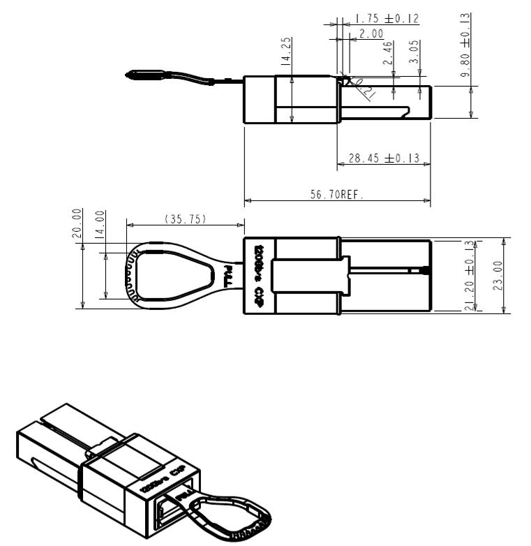
Mechanical Dimensions
Ordering Information
| Part Number | Product Description |
| FTXP-H2-SR10 | CXP Optical Transceivers, 12Channel X 10.5Gb/s, MPO24 OM3 300m 0~70℃ |
| FTXP-H2-SR10I | CXP Optical Transceivers, 12Channel X 10.5Gb/s, MPO24 OM3 300m -40~85℃ |
北亿纤通 | F-tone Networks
企业邮箱: sales@f-tone.com
企业手机:19081343401
企业电话:028-85255257
企业传真:028-85977702
注:本产品有全国产化型号可选
本产品为CXP光模块,仅展示部分参数,如有需要,请联系我们。
Important Notice
Performance figures, data and any illustrative material provided in this data sheet are typical and must be specifically confirmed in writing by F-tone Networks before they become applicable to any particular order or contract. In accordance with the F-tone Networks policy of continuous improvement specifications may change without notice.
The publication of information in this data sheet does not imply freedom from patent or other protective rights of F-tone Networks or others. Further details are available from any F-tone Networks sales representative.
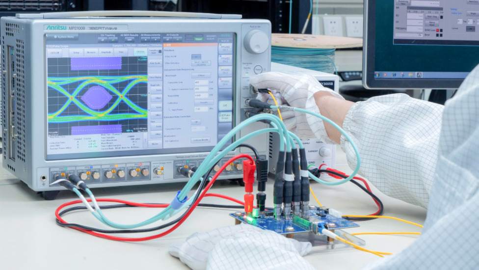
光学性能测试
测试光纤收发模块的眼图情况、接收灵敏度、消光比、波长、发光、光接收、电流和电压,以确保信号质量、传输的稳定性和可靠性。
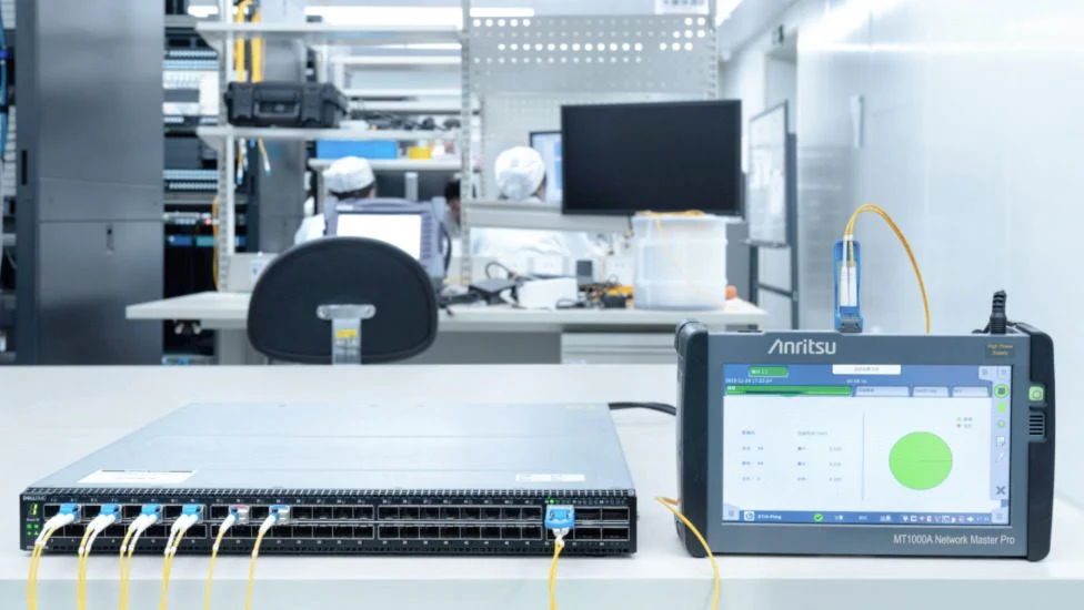
Traffic Testing
测试误码率和丢包率,使其符合相应标准,确保收发器的性能。
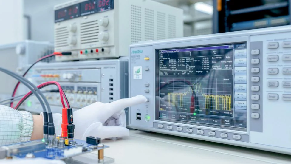
光学性能测试
测试光纤收发模块的眼图情况、接收灵敏度、消光比、波长、发光、光接收、电流和电压,以确保信号质量、传输的稳定性和可靠性。
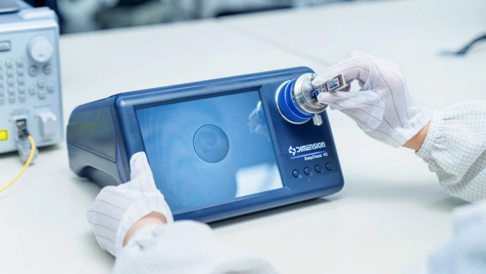
端面测试
检查光纤收发模块的端面并保持清洁,以实现更稳定的数据传输、更好的性能和耐用性。
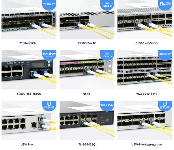
兼容品牌:
华为 | 华三 | 中兴 | 锐捷 | Cisco | Juniper | Arista | Brocade |HPE ProCurve | HPE Aruba | HPE BladeSystem | HPE H3C | H3C | Dell | Extreme | HW | Generic | F-tone | Intel | Netgear | IBM | NVIDIA/Mellanox (Ethernet) | Ciena | Fortinet | Avago | Avaya | Alcatel-Lucent | D-Link | F5 | Ubiquiti | Mikrotik |Broadcom…..