��Ʒ���ࣺ3G/HDSDIģ��
SMPTE 297-2006 compatible
Robust error free transmission of signals from 50Mbps to 3Gbps with up to 30km single-mode fiber
Maximum distance of 10km under worst-case conditions and 3Gbps video pathological signals
Supports video pathological patterns for SD-SDI,HD-SDI and 3G-SDI
SFP Package. Hot-pluggable
Metal enclosure for lower EMI
+3.3V single power supply.
Laser disable pin
Digital diagnostics and control via I²C interface, including:
Monitoring laser bias current, average output power, receive optical power, supply voltage and temperature
Alarm reporting when transceiver is at fault
Module ID polling
Compliant ROHS and lead free
SMPTE 297-2006 compatible optical-to-electrical interfaces
This transceiver is a single channel optical transceiver module designed to transmit and receive optical serial digital signals as defined in SMPTE 297-2006. It is specifically designed for robust performance in the presence of SDI pathological patterns for SMPTE 259M, SMPTE 344M,SMPTE 292M and SMPTE 424M serial rates.
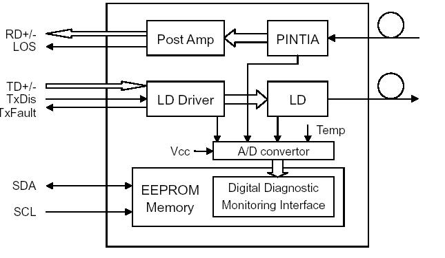
Figure 1: OP-SP13F6-11-SDI Functional Block Diagram
Pin Out Diagram
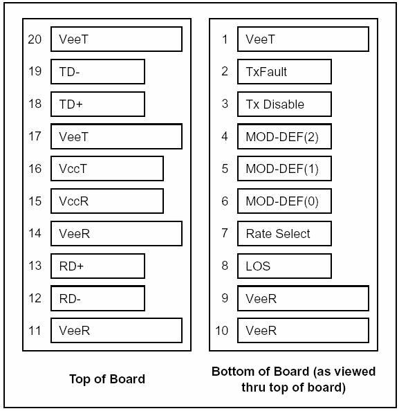
Pin Function Definitions
|
Pin# |
Name |
Description |
Notes |
|
1 |
VEET |
Transmitter Ground |
- |
|
2 |
TX-Fault |
Transmitter Fault Indication |
Note 1 |
|
3 |
TX-Disable |
Transmitter Disable |
Note 2, Module disables on high or open |
|
4 |
SDA |
I²C Data |
Note 3 |
|
5 |
SCL |
I²C Clock |
Note 3 |
|
6 |
Mod-Def |
Module present indicate |
Note 3, Grounded in Module |
|
7 |
NC |
No Connection |
- |
|
8 |
LOS |
Los of signal |
Note 4 |
|
9 |
VEER |
Receiver Ground |
- |
|
10 |
VEER |
Receiver Ground |
- |
|
11 |
VEER |
Receiver Ground |
- |
|
12 |
RD- |
Inv. Received Data Out |
Note 5 |
|
13 |
RD+ |
Receiver Data out |
Note 5 |
|
14 |
VEER |
Receiver Ground |
- |
|
15 |
VCCR |
Receiver Power |
Note 6, 3.3V± 5% |
|
16 |
VCCT |
Transmitter Power |
Note 6, 3.3V± 5% |
|
17 |
VEET |
Transmitter Ground |
- |
|
18 |
TD+ |
Transmit Data In |
Note 7 |
|
19 |
TD- |
Inv. Transmit Data In |
Note 7 |
|
20 |
VEET |
Transmitter Ground |
- |
Note:
Low (0 – 0.8V): Transmitter on
(>0.8, < 2.0V): Undefined
High (2.0 – 3.465V): Transmitter Disabled
Open: Transmitter Disabled
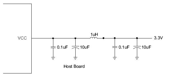
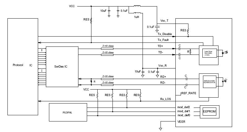
Figure 2: Recommended Host Board Supply Filtering
An LC connector with PC/UPC polish is required for each port.
|
Parameter |
Symbol |
Min. |
Max. |
Unit |
|
Storage Temperature |
TST |
-40 |
+85 |
�� |
|
Operating case Temperature |
Tcase |
-20 |
+85 |
�� |
|
Input Voltage |
- |
GND |
VCC |
V |
|
Power Supply Voltage |
VCC-VEE |
-0.5 |
+3.6 |
V |
|
Parameter |
Symbol |
Min. |
Max. |
Unit |
|
Power Supply Voltage |
VCC |
+3.1 |
+3.5 |
V |
|
Operating Temperature |
To |
0 |
+70 |
�� |
|
Parameter |
Symbol |
Min. |
Typ. |
Max. |
Unit |
Note |
|
Bit Rate |
BR |
50 |
- |
3000 |
Mbps |
- |
|
Center Wavelength |
l |
1290 |
1310 |
1330 |
nm |
- |
|
Spectral Width (RMS) |
Dl |
- |
- |
3 |
nm |
|
|
AverageOptical Output Power |
Po |
-10 |
-6 |
0 |
dBm |
|
|
Extinction Ratio |
ER |
5 |
- |
- |
dB |
- |
|
Power Supply Current |
ICC |
- |
70 |
180 |
mA |
- |
|
Transmitter Enable Voltage |
Ven |
0 |
- |
0.8 |
- |
- |
|
Transmitter disable Voltage |
VD |
2.0 |
- |
VCC |
V |
- |
|
Data Inputs Voltage |
VPP |
300 |
800 |
1600 |
mV |
- |
|
Optical Rise Time (20%~80%) |
Tr |
- |
105 |
165 |
ps |
SMPTE 424M 2.97Gbps |
|
- |
170 |
270 |
ps |
SMPTE 292M 1.485Gbps |
||
|
- |
300 |
800 |
ps |
SMPTE 259M 270Mbps |
||
|
Optical Fall Time (80%~20%) |
Tf |
- |
120 |
180 |
ps |
SMPTE 424M 2.97Gbps |
|
- |
170 |
270 |
Ps |
SMPTE 292M 1.485Gbps |
||
|
- |
300 |
800 |
ps |
SMPTE 259M 270Mbps |
||
|
Optical Signal Intrinsic Jitter |
- |
- |
45 |
70 |
ps |
SMPTE 424M 2.97Gbps |
|
- |
60 |
100 |
ps
|
SMPTE 292M 1.485Gbps
|
||
|
- |
110 |
180 |
ps |
SMPTE 259M 270Mbps |
|
Parameter |
Symbol |
Min. |
Typ. |
Max. |
Unit |
Note |
|
Bit Rate |
BR |
50 |
- |
3000 |
Mbps |
- |
|
Wavelength |
l |
1260 |
- |
1620 |
nm |
- |
|
Saturation |
Ps |
-6 |
- |
- |
dBm |
- |
|
LOS Asserted |
- |
-35 |
- |
- |
dBm |
- |
|
LOS De-Assert |
- |
- |
- |
-20 |
dBm |
- |
|
LOS Hysteresis |
- |
- |
3 |
- |
dB |
- |
|
LOS LOW voltage |
VLout |
- |
- |
0.8 |
V |
- |
|
LOS HIGH voltage |
VHout |
2.0 |
- |
- |
V |
- |
|
Sensitivity for SMPTE 259M 270Mbps |
- |
- |
-22 |
-20 |
dBm |
Pathological |
|
- |
-24 |
-22 |
dBm |
PRBS |
||
|
Sensitivity for SMPTE 292M 1.485Gbps |
- |
- |
-22 |
-20 |
dBm |
Pathological |
|
- |
-24 |
-22 |
dBm |
PRBS |
||
|
Sensitivity for SMPTE 424M 2.97Gbps |
- |
- |
-19 |
-18 |
dBm |
Pathological |
|
- |
-21 |
-20 |
dBm |
PRBS |
||
|
Data Outputs Voltage |
Vpp |
400 |
800 |
1000 |
mV |
- |
|
Input Power Monitoring Accuracy |
|
-1 |
|
+1 |
dB |
- |
Note: The sensitivity specification refers to the input power levels for BER = 1E-12 against PRBS 2 23-1.implemented. The diagnostic data are raw A/D values and must be converted to real world units using calibration constants stored in EEPROM locations 56 – 95 at wire serial bus address A2h. The digital diagnostic memory map specific data field define as following.
Memory Map:
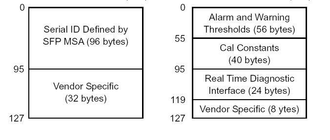
2 wire address 1010000x (A0h) 2 wire address 1010001x (A2h)